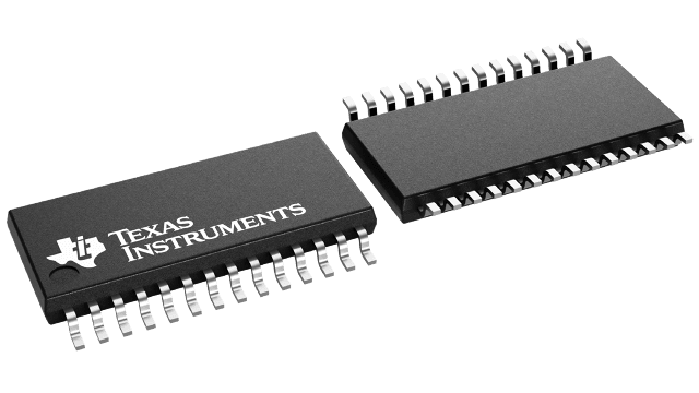
| Function | Memory interface |
| Additive RMS jitter (Typ) (fs) | 30 |
| Output frequency (Max) (MHz) | 667 |
| Number of outputs | 4 |
| Output supply voltage (V) | 2.5 |
| Core supply voltage (V) | 2.5 |
| Output skew (ps) | 15 |
| Features | Spread spectrum clocking (SSC) |
| Operating temperature range (C) | 0 to 70 |
| Rating | Catalog |
| Output type | TTL |
| Input type | TTL |
- High-Speed Clock Support: 300-MHz-667-MHz Clock Source for XDR Memory Subsystems and Redwood Logic Interface
- Quad (Open-Drain) Differential Output Drivers
- Spread-Spectrum Compatible Clock Input Can Be Distributed to Minimize EMI
- Differential or Single-Ended Reference Clock Input of 100 MHz or 133 MHz
- Serial Interface Features: Programmable Frequency Multiplier, Select Any One to Four Outputs and Mode of Operation
- Supports Frequency Multiplication Factors of: ×3, ×4, ×5, ×6, ×8, ×9/2, ×15/2, ×15/4
- All PLL Loop Filter Components Are Integrated
- Low |Cycle-to-Cycle| of 1-6 Cycle Jitter:
- 40 ps: 300-635 MHz
- 30 ps: 636-667 MHz
- PLLs Are Powered Down if No Valid REF Clock (<10 MHz) Is Detected or VDD Is Below 1.6 V
- Operates From Single 2.5-V Supply (±0.125 V)
- Packaged in TSSOP-28
- Commercial Temperature Range 0°C to 70°C
- APPLICATIONS
- XDR Memory Subsystem and Redwood Logic Interface
Rambus, XDR are trademarks of Rambus Inc.
All other trademarks are the property of their respective owners.
The CDCD5704 clock generator provides the necessary clock signals to support an XDR memory subsystem and Redwood logic interface using a reference clock input with or without spread-spectrum modulation. Contained in a 28-pin TSSOP package that includes four differential clock outputs, the CDCD5704 provides an off-the-shelf solution for a broad range of high-performance interface applications.
The block diagram shows the major components of the CDCD5704, which include a phase-locked loop, a bypass multiplexer, and four differential output buffers (CLK0 to CLK3). All four outputs can be disabled by a logical low at the input of the EN pin. An output is enabled when EN is high and a value of 1 is in its serial interface register (RegA-RegD).
The PLL receives a reference clock input signal, REFCLK, and outputs a clock signal at a frequency equal to the input frequency times the multiplication factor. The PLL output clock signal is fed to the differential output buffers to drive the enabled clocks. Disabled outputs are set to high impedance.
The bypass mode routes the input clock REFCLK to the differential output buffers, bypassing the PLL.
To ensure that the CDCD5704 clock generator always performs correctly, the device switches off the PLL and the outputs are in the high-impedance state, once the clock input is below 10 MHz. If the supply voltage VDD is less than VPUC, all logic gates are reset, the PLL is powered down, and the outputs are in the high-impedance state. Therefore, the device only starts its operation if these minimum requirements are met.
Because the CDCD5704 is based on PLL circuitry, it requires a stabilization time to achieve phase-lock of the PLL. With use of an external reference clock, this signal must be fixed-frequency and fixed-phase prior to the start of stabilization time.
The device operates from a single 2.5-V supply voltage. The CDCD5704 device is characterized for operation from 0°C to 70°C.


