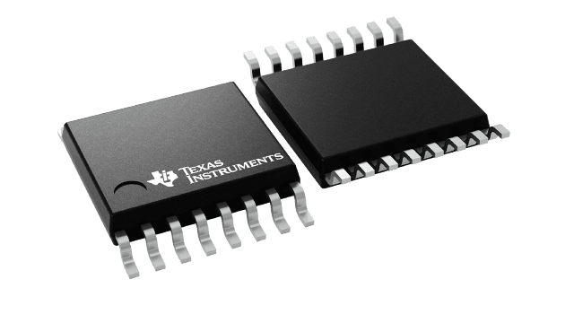
| Resolution (Bits) | 12 |
| Number of DAC channels (#) | 8 |
| Interface type | I2C |
| Output type | Buffered Voltage |
| Settling time (μs) | 7 |
| Features | Cost Optimized, Reset to Mid-Scale, Small Size |
| Reference type | Ext, Int |
| Architecture | String |
| Rating | Catalog |
| Output range (Max) (mA/V) | 5.5 |
| Output range (Min) (mA/V) | 0 |
| Operating temperature range (C) | -40 to 125 |
- Relative Accuracy:
- 1 LSB INL
- Glitch Energy: 0.15nV-s
- Internal Reference:
- 2.5V Reference Voltage (disabled by default)
- ±5mV Initial Accuracy (max)
- 5ppm/°C Temperature Drift (typ)
- 25ppm/°C Temperature Drift (max)
- 20mA Sink/Source Capability
- Power-On Reset to Zero Scale or Midscale
- Devices in the TSSOP Package Reset to
Zero Scale - Devices in the QFN Package Reset to Zero Scale
or Midscale
- Devices in the TSSOP Package Reset to
- Ultra-Low Power Operation: 0.13mA/Channel at 5V
(without internal reference current) - Wide Power-Supply Range: +2.7V to +5.5V
- 2-Wire Serial Interface (I2C compatible)
- On-Chip Output Buffer Amplifier with Rail-to-Rail
Operation - Temperature Range: –40°C to +125°C
- APPLICATIONS
- Portable Instrumentation
- Closed-Loop Servo-Control
- Process Control
- Data Acquisition Systems
- Programmable Attenuation
- PC Peripherals
All other trademarks are the property of their respective owners
The DAC7678 is a low-power, voltage-output, octal channel, 12-bit digital-to-analog converter (DAC). The DAC7678 includes a 2.5V internal reference (disabled by default), giving a full-scale output voltage range of 5V. The internal reference has an initial accuracy of ±5mV and can source up to 20mA at the VREFIN/VREFOUT pin. The device is monotonic, provides very good linearity, and minimizes undesired code-to-code transient voltages (glitch).
The DAC7678 uses a versatile, 2-wire serial interface that is I2C-compatible and operates at clock rates of up to 3.4MHz. Multiple devices can share the same bus.
The DAC7678 incorporates a power-on-reset circuit that ensures the DAC output powers up to either zero-scale or mid-scale until a valid code is written to the device. These devices contain a power-down feature, accessed over the serial interface that reduces the current consumption of the device to typically 0.42μA at 5V. Power consumption (including internal reference) is typically 3.56mW at 3V, reducing to 0.68μW in power-down mode. The low power consumption, internal reference, and small footprint make this device ideal for portable, battery-operated equipment. The DAC7678 is drop-in and functionally compatible with DAC5578, DAC6578, and DAC7578. All devices are available in a 4x4 QFN-24 package and a TSSOP-16 package.


