| Bus voltage (Max) (V) | 110 |
| Power switch | MOSFET |
| Input VCC (Min) (V) | 8 |
| Input VCC (Max) (V) | 17 |
| Peak output current (A) | 3 |
| Rise time (ns) | 8 |
| Operating temperature range (C) | -40 to 125 |
| Undervoltage lockout (Typ) | 8 |
| Rating | Automotive |
| Number of channels (#) | 2 |
| Fall time (ns) | 7 |
| Prop delay (ns) | 20 |
| Iq (uA) | 1 |
| Input threshold | CMOS |
| Channel input logic | CMOS |
| Negative voltage handling at HS pin (V) | -5 |
| Driver configuration | Non-Inverting |
- Qualified for Automotive Applications
- AEC-Q100 Qualified With the Following Results:
- Device Temperature Grade 1:
–40°C to 125°C Ambient Operating Temperature Range - Device HBM ESD Classification Level 2
- Device CDM ESD Classification Level C5
- Device Temperature Grade 1:
- Drives Two N-Channel MOSFETs in High-Side and Low-Side Configuration
- Maximum Boot Voltage: 120 V
- Maximum VDD Voltage: 20 V
- On-Chip 0.65-V VF, 0.6-? RD Bootstrap Diode
- Greater than 1 MHz of Operation
- 20-ns Propagation Delay Times
- 3-A Sink, 3-A Source Output Currents
- 8-ns Rise and 7-ns Fall Time With 1000-pF Load
- 1-ns Delay Matching
- Specified from –40°C to 140°C (Junction Temperature)
All trademarks are the property of their respective owners.
The UCC2720x-Q1 family of high-frequency N-channel MOSFET drivers include a 120-V bootstrap diode and high-side and low-side drivers with independent inputs for maximum control flexibility. This allows for N-channel MOSFET control in half-bridge, full-bridge, two-switch forward, and active-clamp forward converters. The low-side and the high-side gate drivers are independently controlled and matched to 1ns between the turnon and turnoff of each other.
An on-chip bootstrap diode eliminates the external discrete diodes. Undervoltage lockout is provided for both the high-side and the low-side drivers, forcing the outputs low if the drive voltage is below the specified threshold.
Two versions of the UCC2720x-Q1 are offered – the UCC27200-Q1 has high-noise-immune CMOS input thresholds, and the UCC27201-Q1 has TTL-compatible thresholds.
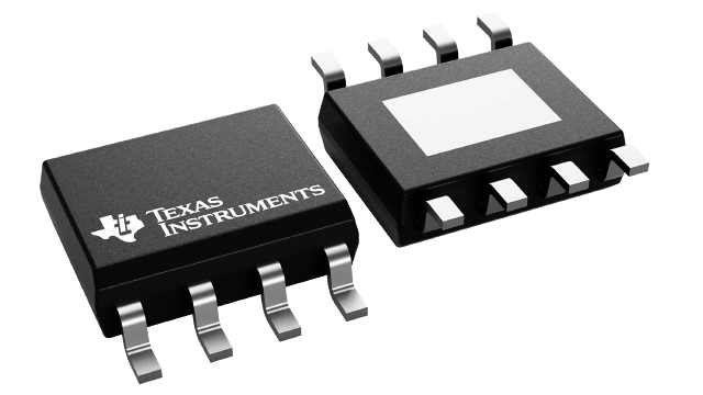
Both devices are offered in the 8-pin SO PowerPAD (DDA) package.
For all available packages, see the orderable addendum at the end of the data sheet.


