
| Bus voltage (Max) (V) | 29 |
| Power switch | MOSFET |
| Input VCC (Min) (V) | 10 |
| Input VCC (Max) (V) | 15 |
| Peak output current (A) | 4 |
| Rise time (ns) | 10 |
| Operating temperature range (C) | -40 to 125 |
| Undervoltage lockout (Typ) | 10 |
| Rating | Catalog |
| Number of channels (#) | 2 |
| Fall time (ns) | 10 |
| Prop delay (ns) | 20 |
| Iq (uA) | 425 |
| Input threshold | TTL |
| Channel input logic | CMOS |
| Negative voltage handling at HS pin (V) | 0 |
| Features | Dead Time Control, Synchronous Rectification |
| Driver configuration | Non-Inverting |
- Integrated Drive Regulator (4 V to 14 V)
- Adjustable/Adaptive Dead-Time Control
- 4-A Peak current at VDRV of 14 V
- 10-V to 15-V Supply Voltage Range
- TTL-Compatible Inputs
- Internal Schottky Diode Reduces Part Count
- Synchronous or Nonsynchronous Operation
- Inverting and Noninverting Options
- TSSOP PowerPad? Package for Excellent Thermal Performance
- APPLICATIONS
- Single or Multiphase Synchronous-Buck Power Supplies
- High-Current DC/DC Power Modules
PowerPAD is a trademark of Texas Instruments.
The TPS2838/39/48/49 devices are MOSFET drivers designed for high-performance synchronous power supplies. The drivers can source and sink up to 4-A peak current at a 14-V drive voltage. These are ideal devices to use with power supply controllers that do not have on-chip drivers. The low-side driver is capable of driving loads of 3.3 nF in 10-ns rise/fall times and has 40-ns propagation delays at room temperature.
The MOSFET drivers have an integrated 150-mA regulator, so the gate drive voltage can be optimized for specific MOSFETs. The TPS2848 and TPS2849 have a fixed 8-V drive regulator, while the TPS2838/39 allow the drive regulator to be adjusted from 4 V to 14 V by selection of two external resistors.
The devices feature VDRV to PGND shoot-through protection with adaptive/adjustable deadtime control. The deadtime, for turning on the high-side FET from LOWDR transitioning low, is adjustable with an external capacitor on the DELAY pin. This allows compensation for the effect the gate resistor has on the synchronous FET turn off. The adaptive deadtime prevents the turning on of the low-side FET until the voltage on the BOOTLO pin falls below a threshold after the high-side FET stops conducting. The high-side drive can be configured as a ground referenced driver or a floating bootstrap driver. The internal Schottky diode minimizes the size and number of external components needed for the bootstrap driver circuit. Only one external ceramic capacitor is required to configure the bootstrap driver.
The SYNC pin can be used regardless of load to disable the synchronous FET driver and operate the power supply nonsynchronously.
A power ready/undervoltage lockout function outputs the status of the VCC-pin voltage and driver regulator output on the open-drain PWRRDY pin. This feature can be used to enable a controller\x92s output once the VCC voltage reaches the threshold and the regulator output is stable. This function ensures both FET drivers are off when the VCC voltage is below the voltage threshold.
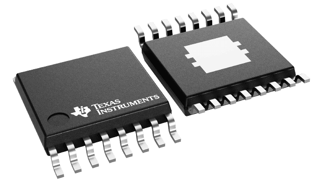
The TPS2838/39/48/49 devices are offered in the thermally enhanced 14-pin and 16-pin PowerPAD TSSOP package. The PowerPAD package features an exposed leadframe on the bottom that can be soldered to the printed-circuit board to improve thermal efficiency. The TPS2838/48 are noninverting control logic while the TPS2839/49 drivers are inverting control logic.


