 電子發(fā)燒友App


Layout Guidelines with Example Layout for the MAX16922 PMIC
Abstract: This application note explains how to layout a standard MAX16922 automotive PMIC (power-management IC) to maximize performance and minimize emissions.
Introduction
When using a high-frequency switching regulator such as the MAX16922, a good PCB layout will provide a clean output supply and save considerable time in the EMI chamber debugging emissions issues. This application note outlines some critical areas of the circuit where optimizing the layout provides the most benefit.
General Layout Guidelines
- For OUT1: minimize the trace loop area for the input capacitor (C1), inductor (L1), catch diode (D1), and output capacitor (C2).
- For OUT2: minimize the trace loop area for the input capacitor (C3), inductor (L2), and output capacitor (C5).
- Connect the power ground (pin 9 and anode of D1) to the rest of the grounds at one point near the exposed pad under the MAX16922. This connection will minimize the noise coupling into the device’s error amplifiers.
- A shorter trace is better than a wider trace.
Optimizing AC-DC Current Paths
The switching regulators of the MAX16922 are the largest source of emissions on the device. Consequently, to minimize emissions, the layout of the passive components of the switching regulators is critical. The paths where there are current-step changes are considered the AC-current paths. These AC-current paths can be seen by eliminating the paths where current flows on both the ON and OFF parts of the switching cycle. The paths that have current flowing through them during the ON and OFF cycles are considered the DC-current paths.
OUT1 AC-Current Path
The DC-DC converter (OUT1) has five passive components (C3, C5, C12, L1, and D1) directly in the switching current path. These five components have the most impact on emissions and performance of OUT1. Figure 1 shows the current path during the ON cycle when the internal DMOS switch is turned on. Figure 2 shows the current path during the OFF cycle when the internal DMOS switch is off. The difference between these two current paths is where the current flow changes suddenly, and is considered the AC-current path (Figure 3). Optimizing the layout of components D1, C3, and C5 is the highest priority, followed by optimizing for components L1 and C12.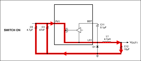
Figure 1. OUT1 current flow with DMOS ON.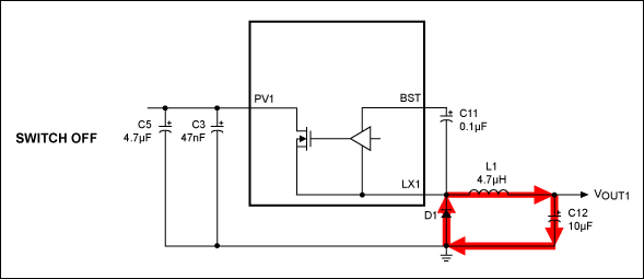
Figure 2. OUT1 current flow with DMOS OFF.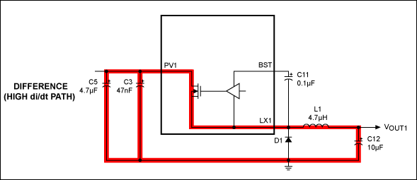
Figure 3. OUT1 AC-current flow showing difference.
OUT2 AC-Current Path
The synchronous DC-DC converter (OUT2) has three passive components (C10, C3, and L2) directly in the switching current path. As with OUT1, these three components have the most impact on emissions and performance of OUT2. Figures 4 and 5 show the switching current path during the ON and OFF cycles; Figure 6 shows the difference between these two current paths where the highest di/dt occurs. Optimizing the layout of component C10 is the highest priority, followed by optimizing for L2 and C13.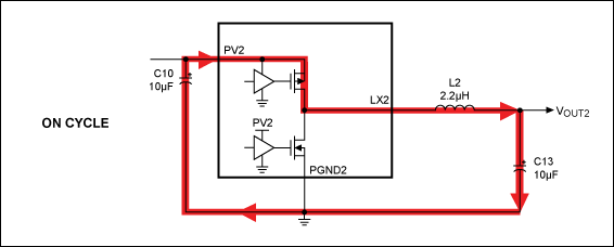
Figure 4. OUT2 current flow with PMOS ON.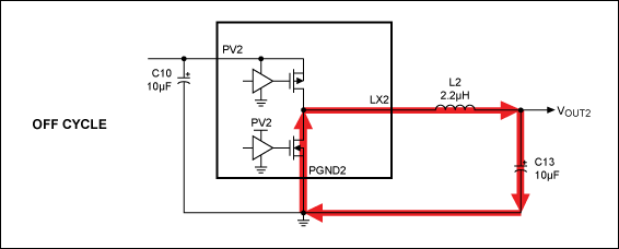
Figure 5. OUT2 current flow with DMOS ON.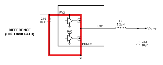
Figure 6, OUT2 AC-current flow showing difference.
OUT1 Boost AC-Current Path
The DC-DC converter (OUT1) uses a high-side DMOS device which requires a supply voltage 5V above the LX1 pin (the source of the DMOS). To generate this voltage a boost capacitor is connected between the LX1 and BST pins (Figure 7). During the OFF cycle of the DMOS, the boost capacitor (C4) is charged from the 5V LSUP regulator. The LSUP output is also used to supply the error amplifiers. It is, therefore, important that LSUP remain as quiet as possible to remove excess noise negatively influencing the error-amplifier circuitry. The best way to accomplish this is to minimize the inductance between the connection to C4 and the MAX16922. Place C4 as close as possible to pin 19 (GND) and pin 17 (LSUP) without adding any vias.
Figure 7. OUT1 boost capacitor AC-current flow.
Adding a Snubber to the LX Node
The rise/fall times of LX1 are as slow as possible to lower the switching noise while not significantly affecting the efficiency of the supply. If further reduction in emissions is required, an RC snubber can be connected to the LX1 pin to dampen the ringing on LX1. It is recommended that the capacitance selected be no more than 330pF so that it does not affect the efficiency significantly and, as is good practice, because it is the smallest capacitor value that gets the job done. A resistance value of around 2Ω is recommended for the resistor. The snubber is marked optional on the schematic diagram in Figure 13 and is comprised of R2 and C13.
The rise/fall times on LX2 are much faster than LX1. Since LX2 is isolated from the main input supply, there are typically no conducted emissions concerns. In some cases, however, the LX2 node can cause emissions issues by radiating to another device and/or connector pins. A snubber can also be added to LX2 to reduce these emissions. Similar value components can be used; the capacitor should be ≤ 220pF along with an 8Ω to 20Ω series resistor.
Example Four-Layer PCB Layout
Figures 8 through Figure 11 show an example of a four-layer layout using the guidelines in this application note. Figure 12 highlights the critical AC- and DC-current paths ON and OFF in the layout.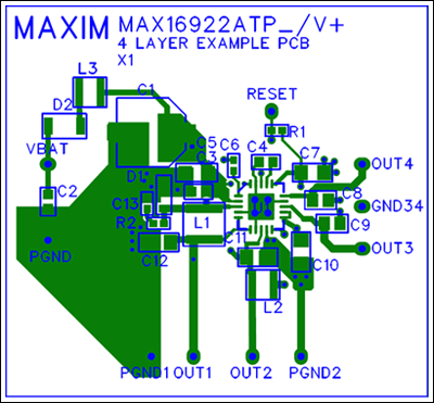
Figure 8. Top layer.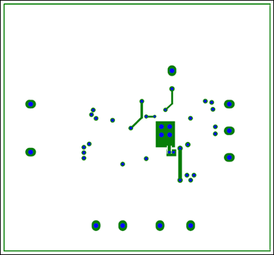
Figure 9. Bottom layer.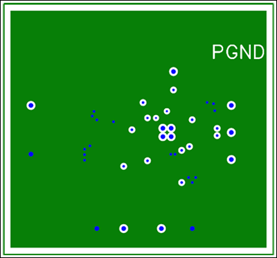
Figure 10. Inner Layer 1, power ground.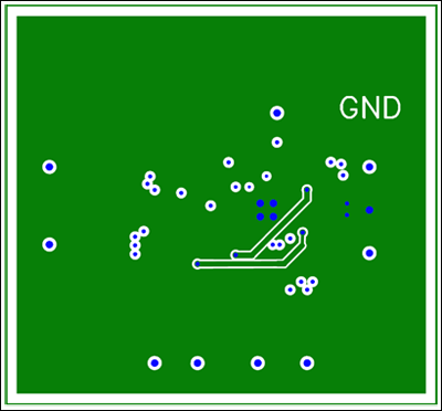
Figure 11. Inner Layer 2, ground.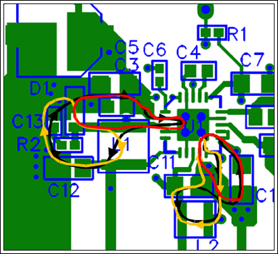
Figure 12. Current paths: black Is the ON cycle; orange Is the OFF cycle; red Is the difference.
Main Supply Filtering
The filtering on the main supply is also very important, as this is the last point at which conducted emissions can be reduced before exiting the module. For high-frequency switching regulators such as the MAX16922, conducted emissions issues usually occur in the FM radio band (76MHz to 108MHz). To reduce these emissions add a ferrite bead with high impedance in this frequency range, and/or an inductor with a self-resonant frequency above 108MHz.
Conclusion
Proper layout of the critical passive components for the switching regulators of the MAX16922 will help to minimize the noise and emissions at the source. This will save valuable time and effort during the qualification phase of the project.
Table 1. Component List
| Designation | Qty | Description |
| C1 | 1 | 47μF, 25V electrolytic capacitor |
| C2–C3 | 2 | 47nF, 50V ±10% X7R 0603 ceramic capacitors |
| C4 | 1 | 1μF, 10V ±10% X7R 0603 ceramic capacitor |
| C5 | 1 | 4.7μF, 50V ±10% X7R 1210 ceramic capacitor |
| C6 | 1 | 100nF, 10V ±10% X7R 0402 ceramic capacitor |
| C7 | 1 | 4.7μF, 10V ±10% X7R 1206 ceramic capacitor |
| C8–C9 | 2 | 2.2μF, 10V ±10% X7R 0805 ceramic capacitors |
| C10–C12 | 3 | 10μF, 10V ±10% X7R 1206 ceramic capacitors |
| C13 | 1 | 100pF, 50V ±10% X7R 0402 ceramic capacitor |
| R1 | 1 | 20kΩ ±1% 0402 resistor |
| R2 | 1 | 2Ω ±5% 0402 resistor |
| L1 | 1 | 4.7μH inductor |
| L2–L3 | 2 | 2.2 μH inductors |
| D1 | 1 | MBR140SFT1 Schottky diode |
| D2 | 1 | ES1D diode |
| U1 | 1 | MAX16922ATPA/V+ quad-output PMIC |
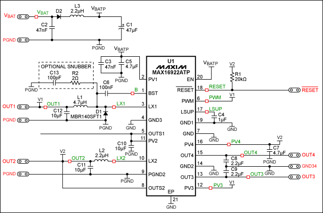
Figure 13. Schematic diagram used for PCB layouts.


 工商網(wǎng)監(jiān)
評(píng)論