 電子發(fā)燒友App


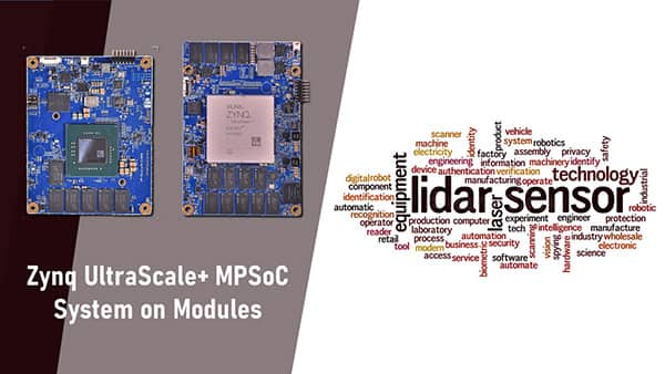
Avnet公司的Ultra96 開發(fā)板是基于ARM的Xilinx ZynqUltraScale+? MPSoC系列產(chǎn)品的滿足Linaro 96板指標(biāo)的開發(fā)板,設(shè)計(jì)者可創(chuàng)建或評估Zynq處理器子系統(tǒng)(PS)和可編邏輯(PL)架構(gòu),主要用在航空航天與國防,汽車電子,數(shù)據(jù)中心,無線通信基礎(chǔ)設(shè)備和無線基礎(chǔ)設(shè)施.本文介紹了Xilinx公司的Zynq? UltraScale+?MPSoC系列主要特性,應(yīng)用方案以及AvnetUltra96開發(fā)板主要特性,框圖,電路圖,材料清單和PCB設(shè)計(jì)圖.
Zynq? UltraScale+? All Programmable MPSoCs provide up to 5X systemlevelperformance-per-watt compared to the Zynq-7000 SoC family.
ZynqUltraScale+ devices combine a high-performance ARM?-basedmulticore,multiprocessing system with ASIC-class programmable logic.
Dual- and quad-core application processor equipped devices delivermaximum scalability, and are capable of offloading critical applications,such as graphics and video pipelining, to dedicated processing blocks,along with a full complement of integrated peripherals and connectivitycores suitable for next-generation systems.
For the most compute intensive processing tasks, integratedprogrammable logic offers up to 100X performance improvement overprocessor-based implementations. The 16nm FinFET+ programmablelogic communicates with the processing system through 6,000 interconnects, enabling bandwidth that is not possible with multichipsolutions. Dramatic power savings are achieved through fine-grainedcontrol of power domains and gated power islands. With specializedprocessing elements for different workloads, ZynqUltraScale+ MPSoCsintegrate the right engines for the right tasks for next-generation
embedded challenges.
Ultra96? is an Arm-based, Xilinx ZynqUltraScale+? MPSoC development board based on the Linaro 96Boards specification.
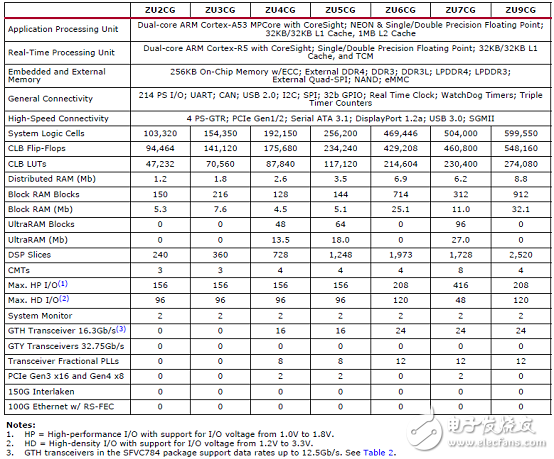
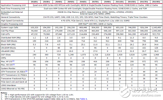
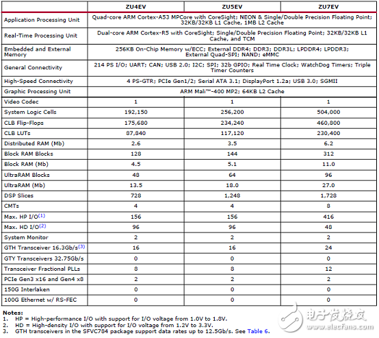
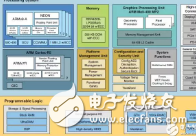
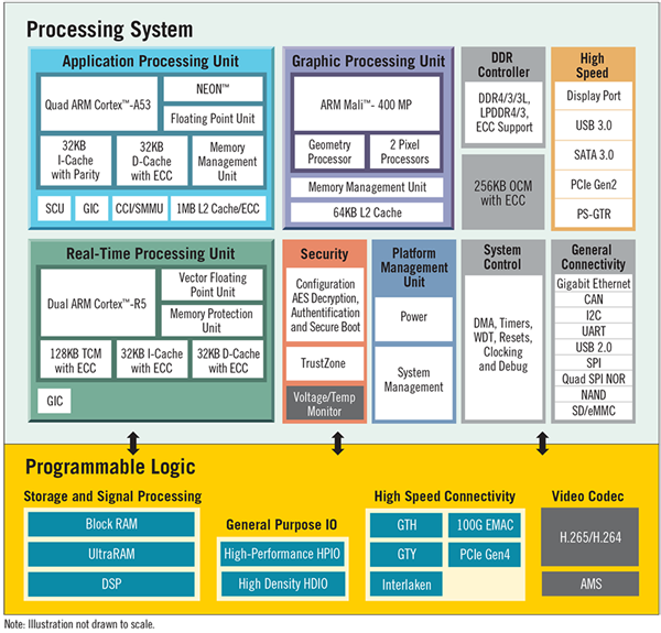
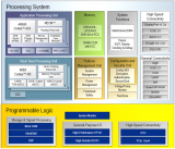
The Zynq? UltraScale+? MPSoC family is based on the Xilinx? UltraScale? MPSoC architecture. Thisfamily of products integrates a feature-rich 64-bit quad-core or dual-core ARM? Cortex?-A53 anddual-core ARM Cortex-R5 based processing system (PS) and Xilinx programmable logic (PL)UltraScalearchitecture in a single device. Also included are on-chip memory, multiport external memory interfaces,and a rich set of peripheral connectivity interfaces.
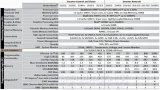
Zynq? UltraScale+? MPSoC系列主要特性:
Processing System (PS)
ARM Cortex-A53 Based ApplicationProcessing Unit (APU)
? Quad-core or dual-core
? CPU frequency: Up to 1.5GHz
? Extendable cache coherency
? ARMv8-A Architecture
o 64-bit or 32-bit operating modes
oTrustZone security
o A64 instruction set in 64-bit mode,A32/T32 instruction set in 32-bit mode
? NEON Advanced SIMD media-processing engine
? Single/double precision Floating Point Unit (FPU)
? CoreSight? and Embedded Trace Macrocell (ETM)
? Accelerator Coherency Port (ACP)
? AXI Coherency Extension (ACE)
? Power island gating for each processor core
? Timer and Interrupts
o ARM Generic timers support
o Two system level triple-timer counters
o One watchdog timer
o One global system timer
? Caches
o 32KB Level 1, 2-way set-associativeinstruction cache with parity (independent for
each CPU)
o 32KB Level 1, 4-way set-associative datacache with ECC (independent for each CPU)
o 1MB 16-way set-associative Level 2 cachewith ECC (shared between the CPUs)
Dual-core ARM Cortex-R5 BasedReal-Time Processing Unit (RPU)
? CPU frequency: Up to 600MHz
? ARMv7-R Architecture
o A32/T32 instruction set
? Single/double precision Floating Point Unit (FPU)
? CoreSight? and Embedded Trace Macrocell(ETM)
? Lock-step or independent operation
? Timer and Interrupts:
o One watchdog timer
o Two triple-timer counters
? Caches and Tightly Coupled Memories (TCMs)
o 32KB Level 1, 4-way set-associativeinstruction and data cache with ECC
(independent for each CPU)
o 128KB TCM with ECC (independent for eachCPU) that can be combined to become 256KBin lockstep mode
On-Chip Memory
? 256KB on-chip RAM (OCM) in PS with ECC
? Up to 36Mb on-chip RAM (UltraRAM) with ECC inPL
? Up to 35Mb on-chip RAM (block RAM) with ECCin PL
? Up to 11Mb on-chip RAM (distributed RAM) in PL
ARM Mali-400 Based GPU
? Supports OpenGL ES 1.1 and 2.0
? Supports OpenVG 1.1
? GPU frequency: Up to 667MHz
? Single Geometry Processor, Two Pixel Processors
? Pixel Fill Rate: 2 Mpixels/sec/MHz
? Triangle Rate: 0.11 Mtriangles/sec/MHz
? 64KB L2 Cache
? Power island gating
External Memory Interfaces
? Multi-protocol dynamic memory controller
? 32-bit or 64-bit interfaces to DDR4, DDR3,DDR3L, or LPDDR3 memories, and 32-bit
interface to LPDDR4 memory
? ECC support in 64-bit and 32-bit modes
? Up to 32GB of address space using single or dualrank of 8-, 16-, or 32-bit-wide memories
? Static memory interfaces
o eMMC4.51 Managed NAND flash support
o ONFI3.1 NAND flash with 24-bit ECC
o 1-bit SPI, 2-bit SPI, 4-bit SPI (Quad-SPI), ortwo Quad-SPI (8-bit) serial NOR flash
8-Channel DMA Controller
? Two DMA controllers of 8-channels each
? Memory-to-memory, memory-to-peripheral,peripheral-to-memory, and scatter-gather transaction support
Serial Transceivers
? Four dedicated PS-GTR receivers andtransmitters supports up to 6.0Gb/s data rates
o Supports SGMII tri-speed Ethernet, PCIExpress? Gen2, Serial-ATA (SATA), USB3.0,and DisplayPort Dedicated I/O Peripherals andInterfaces
? PCI Express — Compliant with PCIe? 2.1 basespecification
o Root complex and End Point configurations
o x1, x2, and x4 at Gen1 or Gen2 rates
? SATA Host
o 1.5, 3.0, and 6.0Gb/s data rates as defined bySATA Specification, revision 3.1
o Supports up to two channels
? DisplayPort Controller
o Up to 5.4Gb/s rate
o Up to two TX lanes (no RX support)
? Four 10/100/1000 tri-speed Ethernet MACperipherals with IEEE Std 802.3 and IEEE Std 1588revision 2.0 support
o Scatter-gather DMA capability
o Recognition of IEEE Std 1588 rev.2 PTP frames
o GMII, RGMII, and SGMII interfaces
o Jumbo frames
? Two USB 3.0/2.0 Device, Host, or OTG peripherals,each supporting up to 12 endpoints
o USB 3.0/2.0 compliant device IP core
o Super-speed, high- speed, full-speed, andlow-speed modes
o Intel XHCI- compliant USB host
? Two full CAN 2.0B-compliant CAN bus interfaces
o CAN 2.0-A and CAN 2.0-B and ISO 118981-1standard compliant
? Two SD/SDIO 2.0/eMMC4.51 compliantcontrollers
? Two full-duplex SPI ports with three peripheralchip selects
? Two high-speed UARTs (up to 1Mb/s)
? Two master and slave I2C interfaces
? Up to 78 flexible multiplexed I/O (MIO) (up tothree banks of 26 I/Os) for peripheral pin
assignment
? Up to 96 EMIOs (up to three banks of 32 I/Os)connected to the PL
Interconnect
? High-bandwidth connectivity within PSand between PS and PL
? ARM AMBA? AXI4-based
? QoS support for latency and bandwidth control
? Cache Coherent Interconnect (CCI)
System Memory Management
? System Memory Management Unit (SMMU)
? Xilinx Memory Protection Unit (XMPU)
Platform Management Unit
? Power gates PS peripherals, power islands, andpower domains
? Clock gates PS peripheral user firmware option
Configuration and Security Unit
? Boots PS and configures PL
? Supports secure and non-secure boot modes
System Monitor in PS
? On-chip voltage and temperature sensing
Programmable Logic (PL)
Configurable Logic Blocks (CLB)
? Look-up tables (LUT)
? Flip-flops
? Cascadable adders
36Kb Block RAM
? True dual-port
? Up to 72 bits wide
? Configurable as dual 18Kb
UltraRAM
? 288Kb dual-port
? 72 bits wide
? Error checking and correction
DSP Blocks
? 27 x 18 signed multiply
? 48-bit adder/accumulator
? 27-bit pre-adder
Programmable I/O Blocks
? Supports LVCMOS, LVDS, and SSTL
? 1.0V to 3.3V I/O
? Programmable I/O delay and SerDes
JTAG Boundary-Scan
? IEEE Std 1149.1 Compatible Test Interface
PCI Express
? Supports Root complex and End Pointconfigurations
? Supports up to Gen4 speeds
? Up to five integrated blocks in select devices
100G Ethernet MAC/PCS
? IEEE Std 802.3 compliant
? CAUI-10 (10x 10.3125Gb/s) or
CAUI-4 (4x 25.78125Gb/s)
? RSFEC (IEEE Std 802.3bj) in CAUI-4 configuration
? Up to four integrated blocks in select devices
Interlaken
? Interlaken spec 1.2 compliant
? 64/67 encoding
? 12 x 12.5Gb/s or 6 x 25Gb/s
? Up to four integrated blocks in select devices
Video Encoder/Decoder (VCU)
? Available in EV devices
? Accessible from either PS or PL
? Simultaneous encode and decode
? H.264 and H.265 support
System Monitor in PL
? On-chip voltage and temperature sensing
? 10-bit 200KSPS ADC with up to 17 external inputs
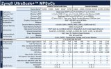
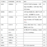
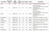
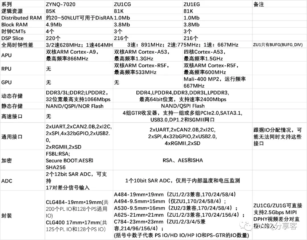
ZynqUltraScale+ MPSoC: CG器件主要特性:
ZynqUltraScale+ MPSoC: EG器件主要特性:
ZynqUltraScale+ MPSoC: EV器件主要特性:
ZynqUltraScale+ MPSoC系列目標(biāo)應(yīng)用:
? Aerospace & Defense
? Automotive
? Data Center
? Wired Communications Infrastructure
? Wireless Infrastructure
應(yīng)用案例1:
基于照相機(jī)的高檔輔助駕駛系統(tǒng)(ADAS)
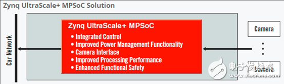
? Quad-core ARM Cortex-A53 for vision analytics, streaming, and automated metadata
? Dual-core ARM Cortex-R5 for real-time peripheral interfaces
? Advanced power management, power islands, and lock-step mode with real-time processing for functional safety
? Video encoder/decoder, supporting H.265/H.264 for display connectivity
? CAN2.0B and Gigabit Ethernet support for IEEE Std 1588 and AVB for in-vehicle communications
應(yīng)用案例2:
公共安全和軍用移動(dòng)無線電:
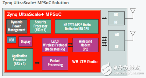
? Platform Management Unit (PMU) to dynamically lower power, maximizing battery life
? Quad-core ARM Cortex-A53 to integrate application processing and radio modem
? Vivado HLS and SDx? Design Environment for high-level (C/C++) waveform development
? W-Mux DSP48 for efficient complex filter implementation
? Processing System (PS) with varying Programmable Logic (PL) for radio scalability with maximum software reuse
? Dedicated configuration security unit (CSU) for security management
Avnet Ultra96? is an Arm-based, Xilinx ZynqUltraScale+? MPSoC development board based on the Linaro 96Boards specification.
The Avnet Ultra96 enables hardware and software developers to explore the capabilities of the Zynq? UltraScale+? MPSoC. Designers can create or evaluate designs for both the Zynq Processor Subsystem (PS) and the Programmable Logic (PL) fabric
圖1.Ultra96開發(fā)板外形圖
Ultra96開發(fā)板主要特性:
? ZynqUltraScale+ MPSoC ZU3EG SBVA484
? Memory
oMicron 2 GB (512M x32) LPDDR4 Memory
oMiroSD Socket
§ Ships with Delkin Utility MLC 16GB card
? Wi-Fi / Bluetooth
? DisplayPort
? 1x USB 3.0 Type Micro-B upstream port
? 2x USB 3.0 Type A downstream ports
? 40-pin Low-speed expansion header
? 60-pin High speed expansion header
? Mounted on thermal bracket with fan
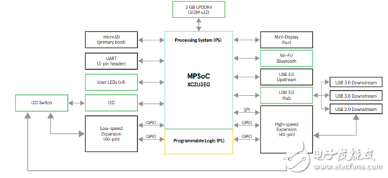
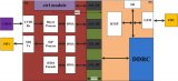
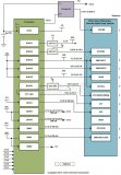
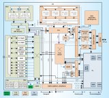
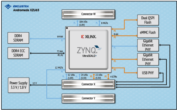
圖2.Ultra96開發(fā)板框圖
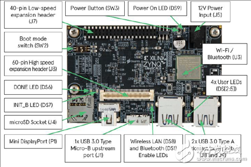
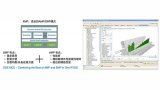
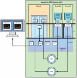
圖3.Ultra96開發(fā)板拓?fù)鋱D
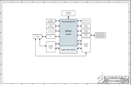
圖4.Ultra96開發(fā)板電路圖(1)
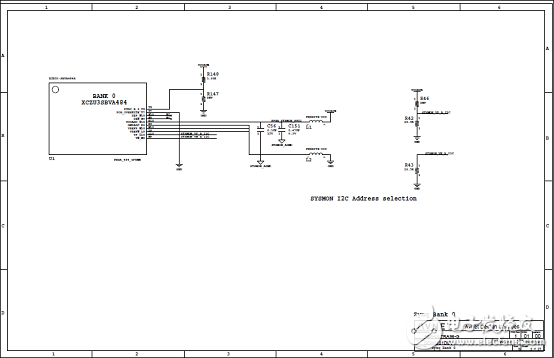
圖5.Ultra96開發(fā)板電路圖(2)
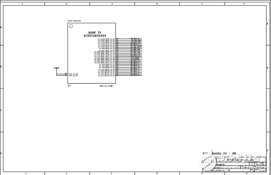
圖6.Ultra96開發(fā)板電路圖(3)
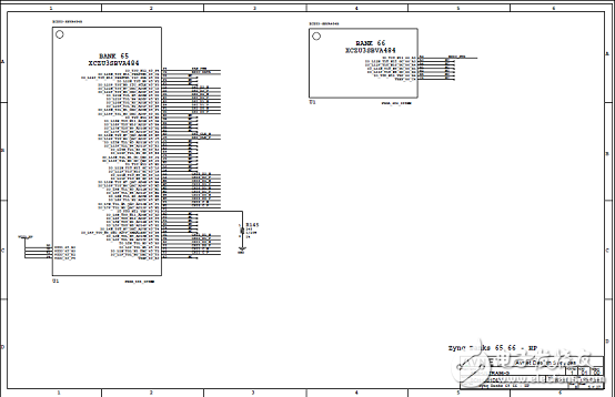
圖7.Ultra96開發(fā)板電路圖(4)
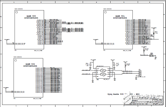
圖8.Ultra96開發(fā)板電路圖(5)
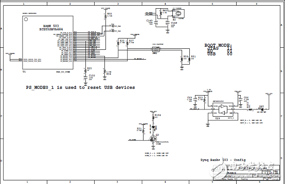
圖9.Ultra96開發(fā)板電路圖(6)
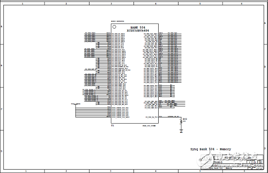
圖10.Ultra96開發(fā)板電路圖(7)

圖11.Ultra96開發(fā)板電路圖(8)
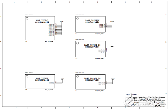
圖12.Ultra96開發(fā)板電路圖(9)
圖13.Ultra96開發(fā)板電路圖(10)
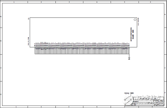
圖14.Ultra96開發(fā)板電路圖(11)
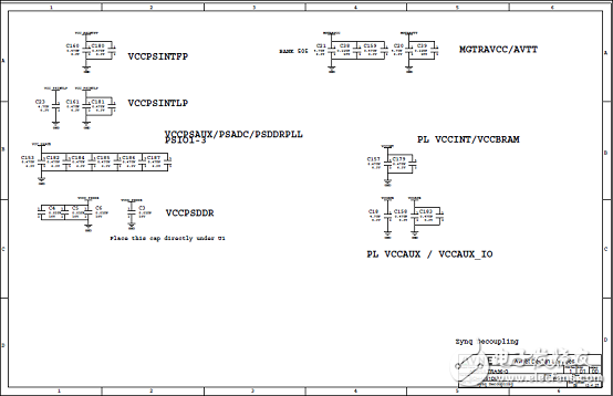
圖15.Ultra96開發(fā)板電路圖(12)
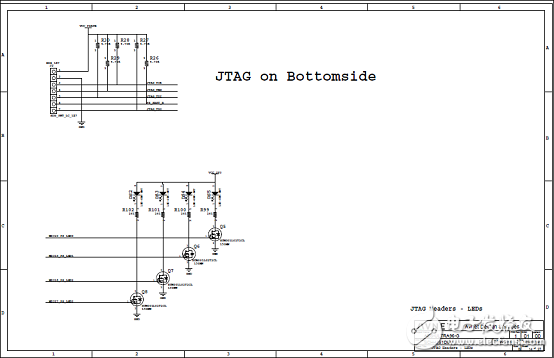
圖16.Ultra96開發(fā)板電路圖(13)

圖17.Ultra96開發(fā)板電路圖(14)

圖18.Ultra96開發(fā)板電路圖(15)
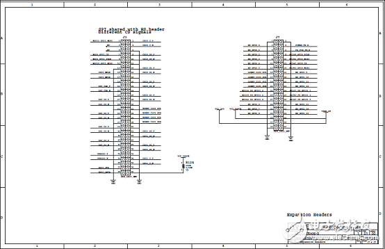
圖19.Ultra96開發(fā)板電路圖(16)
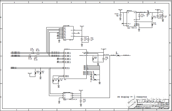
圖20.Ultra96開發(fā)板電路圖(17)
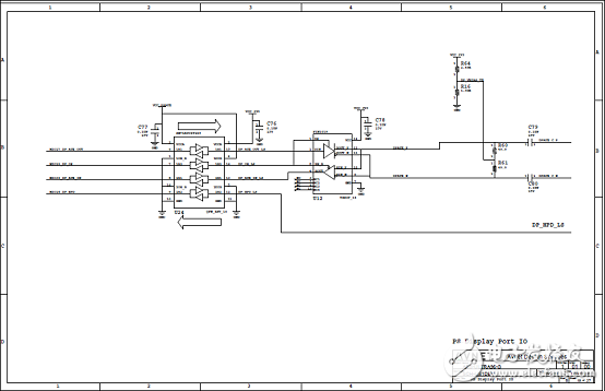
圖21.Ultra96開發(fā)板電路圖(18)
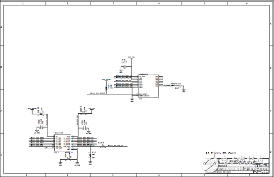
圖22.Ultra96開發(fā)板電路圖(19)
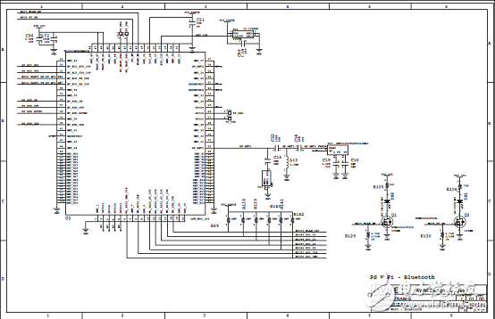
圖23.Ultra96開發(fā)板電路圖(20)
![[原創(chuàng)] Avnet Zynq UltraScale+MPSoC系列Ultra96開發(fā)方案](/uploads/allimg/181201/1K60193K_0.png)
圖24.Ultra96開發(fā)板電路圖(21)
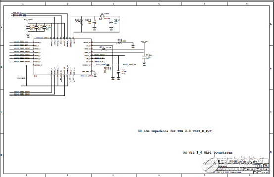
圖25.Ultra96開發(fā)板電路圖(22)
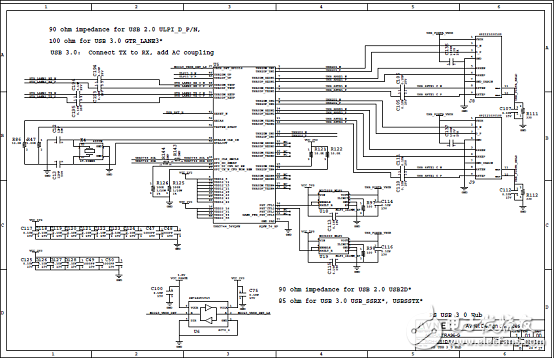
圖26.Ultra96開發(fā)板電路圖(23)
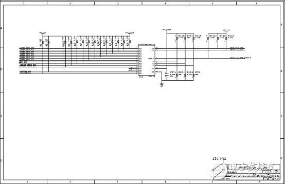
圖27.Ultra96開發(fā)板電路圖(24)
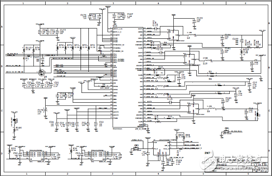
圖28.Ultra96開發(fā)板電路圖(25)
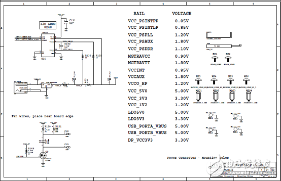
圖29.Ultra96開發(fā)板電路圖(26)
Ultra96開發(fā)板材料清單:

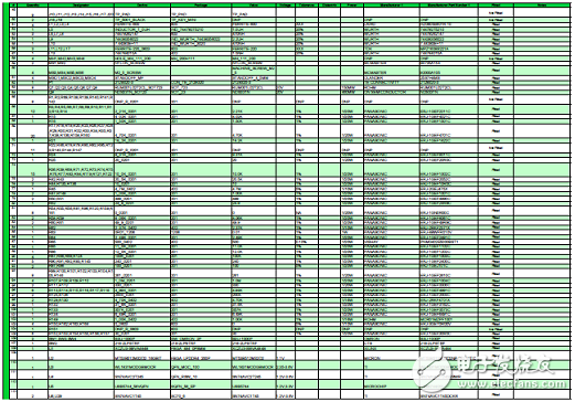
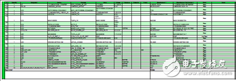

圖30.Ultra96開發(fā)板PCB設(shè)計(jì)圖(1)

圖31.Ultra96開發(fā)板PCB設(shè)計(jì)圖(2)
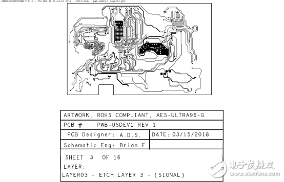
圖32.Ultra96開發(fā)板PCB設(shè)計(jì)圖(3)
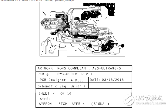
圖33.Ultra96開發(fā)板PCB設(shè)計(jì)圖(4)
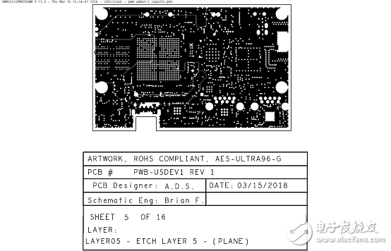
圖34.Ultra96開發(fā)板PCB設(shè)計(jì)圖(5)
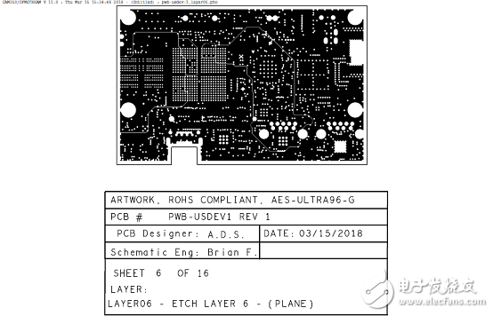
圖35.Ultra96開發(fā)板PCB設(shè)計(jì)圖(6)
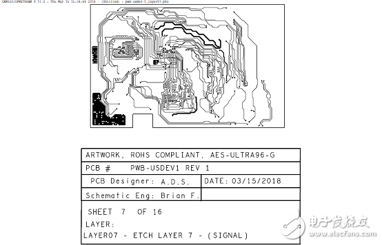
圖36.Ultra96開發(fā)板PCB設(shè)計(jì)圖(7)
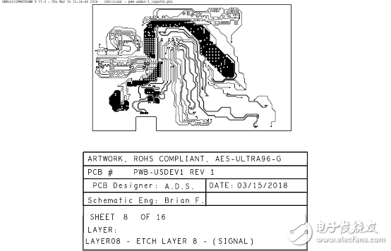
圖37.Ultra96開發(fā)板PCB設(shè)計(jì)圖(8)
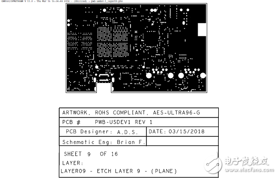
圖38.Ultra96開發(fā)板PCB設(shè)計(jì)圖(9)
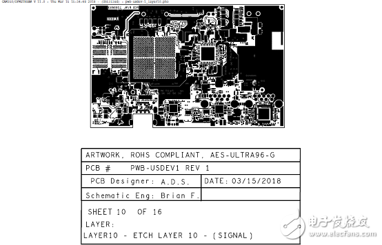
圖39.Ultra96開發(fā)板PCB設(shè)計(jì)圖(10)
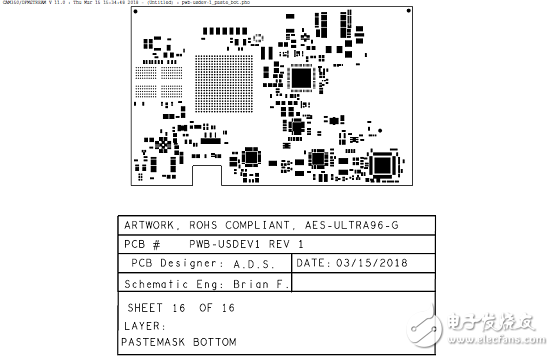
圖40.Ultra96開發(fā)板PCB設(shè)計(jì)圖(11)
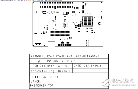
圖41.Ultra96開發(fā)板PCB設(shè)計(jì)圖(12)
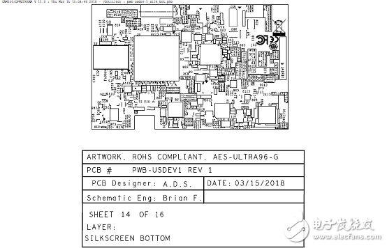
圖42.Ultra96開發(fā)板PCB設(shè)計(jì)圖(13)
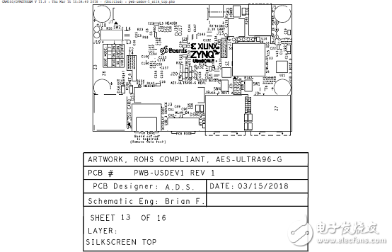
圖44.Ultra96開發(fā)板PCB設(shè)計(jì)圖(15)
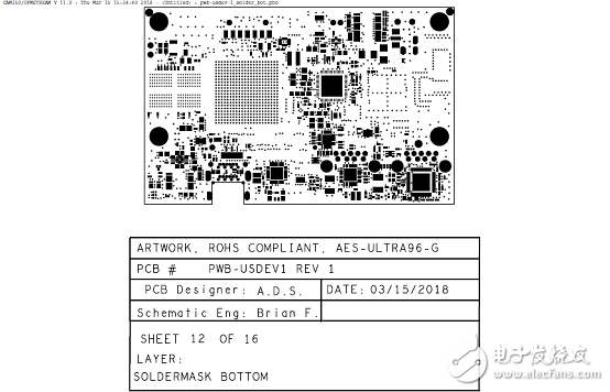
圖45.Ultra96開發(fā)板PCB設(shè)計(jì)圖(16)
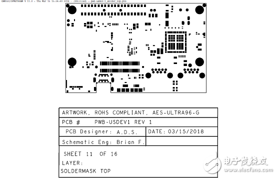
圖46.Ultra96開發(fā)板PCB設(shè)計(jì)圖(17)


 工商網(wǎng)監(jiān)
評論